Gebäude von Telefon- und Internetgeräten: Ein vollständiger Leitfaden
Einleitung: Grundlegendes Verständnis
Der Bau von Telekommunikationsgeräten erfordert sorgfältige Technik. Es ist viel mehr als nur das Platzieren von Teilen auf einer Leiterplatte. Es ist ein detaillierter Prozess, der strengen Regeln folgt, bei dem Erfolg von klaren Signalen, stabilen Temperaturen und langlebiger Zuverlässigkeit abhängt. Ein kleiner Fehler kann eine Netzwerkinstallation im Wert von Millionen von Euro ruinieren. Dieser Leitfaden erklärt die wichtigsten Teile, die die Montage moderner, hochwertiger Telekommunikationsgeräte ausmachen.
Wir werden dieses komplexe Gebiet aufschlüsseln, indem wir seine Grundbestandteile betrachten. Das deckt dieser Leitfaden ab:
- Herstellung von Leiterplatten und Materialien
- Auswahl und Platzierung von Komponenten
- Fortgeschrittene Löt- und Verbindungstechniken
- Wichtige Strategien zum Wärmemanagement
- Funkfrequenzabschirmung und Prinzipien der Signalqualität
- Vollständig Qualitätskontrolle und Tests Verfahren
Dieser detaillierte Leitfaden richtet sich an Ingenieure und technische Fachkräfte, die verstehen müssen, wie Rohteile zu zuverlässiger, leistungsstarker Hardware werden, die globale Kommunikationsnetze antreibt.
Warum technische Analyse wichtig ist
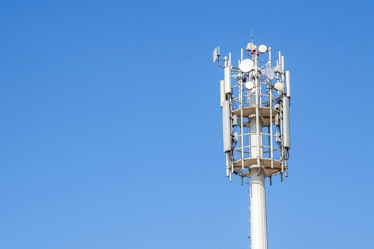
Die Bedeutung der Montage von Telekommunikationsgeräten ist enorm. Ein Mobilfunkturm, ein Hauptrouter oder ein optischer Schalter ist kein Konsumgerät; es ist kritische Infrastruktur, die erwartet wird, jahrelang perfekt zu funktionieren, oft unter schwierigen Umweltbedingungen. Schlechte Montage führt direkt zu größeren Ausfällen: Signale, die Anrufe abbrechen und Daten verlangsamen, Überhitzung, die Komponenten frühzeitig zerstört, und Störungsprobleme, die die Netzstabilität beeinträchtigen. Das Verständnis der technischen Details des Montageprozesses ist entscheidend, um die Leistung der Geräte und die Zuverlässigkeit des Netzwerks zu gewährleisten.
Der Umfang unserer Analyse
Um eine vollständige Übersicht zu bieten, werden wir unsere Analyse logisch organisieren, beginnend mit grundlegenden Konzepten bis hin zu fortgeschrittenen Anwendungen und Überprüfungen.
- Grundlagen: Wir beginnen mit der Anatomie der Telekommunikationshardware und identifizieren die wichtigsten Komponenten.
- Kernprozesse: Wir untersuchen dann die wichtigsten Montagetechnologien und die Materialwissenschaft hinter sie.
- Tiefenanalyse: Wir konzentrieren uns auf die kritischsten technischen Herausforderungen: Wärme management, Signalintegrität bewahren und Störungen reduzieren.
- Verifikation: Wir behandeln die wesentlichen Qualitätssicherungs- und Testverfahren, die den Montageprozess validieren.
- Zukunftsausblick: Schließlich blicken wir auf die aufkommenden Trends, die die Zukunft der Telekommunikationsmontage prägen.
Anatomie von Telekommunikationsgeräten
Bevor wir untersuchen, wie Telekommunikationsgeräte gebaut werden, müssen wir zuerst verstehen, woraus sie bestehen. Moderne Telekommunikationshardware, von einer 5G-Radiostation bis zu einem Rechenzentrum-Switch, ist ein komplexes System aus spezialisierten Komponenten, die auf einer zentralen Plattform integriert sind.
Das zentrale Nervensystem: PCBAs
Die Leiterplattenmontage (PCBA) ist das Rückgrat jedes elektronischen Geräts. Sie bietet sowohl die physische Struktur für die Montage der Komponenten als auch das komplexe Netzwerk leitfähiger Wege, die deren Kommunikation ermöglichen. Im Telekommunikationssektor sind dies keine Standard-Leiterplatten. Sie sind oft komplexe, mehrlagige Platinen – manchmal mit 20 oder mehr Schichten – die spezielle Materialien verwenden, um Hochfrequenzsignale mit minimalem Verlust zu handhaben. Der gesamte Montageprozess folgt strengen Standards wie IPC-A-610, die die Qualitätskriterien für elektronische Baugruppen definieren und eine Grundqualität sowie Zuverlässigkeit sicherstellen.
Kernverarbeitung und Logik
Im Herzen jedes Telekommunikationsgeräts stehen die Komponenten, die Daten mit unglaublicher Geschwindigkeit verarbeiten.
- Anwendungsspezifische integrierte Schaltkreise (ASICs): Diese sind kundenspezifische Siliziumchips, die von Grund auf so entwickelt wurden, dass sie eine einzelne, hochspezialisierte Funktion ausführen, wie Paketweiterleitung oder digitale Signalverarbeitung. Ihr festes Design liefert maximale Leistung und Energieeffizienz für eine bekannte Arbeitsbelastung.
- Feldprogrammierbare Gate-Arrays (FPGAs): Diese Chips bieten eine leistungsstarke Alternative zu ASICs. Sie enthalten eine Matrix konfigurierbarer Logikblöcke, die im Feld programmiert werden können, was eine entscheidende Flexibilität bietet, um sich an neue Protokolle oder sich entwickelnde Standards anzupassen, ohne eine Hardware-Neuentwicklung.
- Netzprozessoren (NPUs): Diese sind hochspezialisierte Mikroprozessoren mit Architekturen, die für die in der Netzwerktechnik üblichen Operationen optimiert sind, wie Paketinspektion und Verkehrsmanagement. Sie verbinden die Leistung von ASICs mit der Programmierbarkeit von allgemeinen CPUs.
RF- und optische Komponenten
Diese Komponenten bilden die Brücke zwischen der digitalen Verarbeitung und dem physischen Übertragungsmedium, sei es Funkwellen oder Glasfaserkabel.
- Funkfrequenz (RF)-Komponenten: Diese Familie umfasst RF-Transceiver, die digitale Daten in analoge Funksignale umwandeln und umgekehrt; Leistungsverstärker (PAs), die das Signal für die Übertragung verstärken; und Rauschverstärker (LNAs), die schwache eingehende Signale verstärken, ohne erhebliches Rauschen einzuführen.
- Optische Transceiver: Diese Module wandeln elektrische Signale in Licht für die Übertragung über Glasfaserkabel und wieder zurück. Gängige Formfaktoren wie SFP (Small Form-factor Pluggable) und QSFP (Quad Small Form-factor Pluggable) sind in moderner Telekommunikation und Rechenzentrumsausrüstung üblich. Während der Montage erfordern diese Komponenten äußerst sorgfältige Handhabung, um empfindliche RF-Wege und delicate optische Schnittstellen zu schützen.
Stromversorgungssysteme und Mechanik
Zur Unterstützung der Hochleistungs-Elektronik gehören die Strom- und mechanischen Systeme. Dazu gehören spezielle Netzteile (PSUs), die stabile, saubere Energie an alle Komponenten liefern, sowie die verschiedenen Anschlüsse für Daten und Strom. Das mechanische Gehäuse oder Chassis ist viel mehr als nur eine einfache Box. Es ist ein integraler Bestandteil des Systems, der so konstruiert ist, dass er strukturelle Unterstützung bietet, eine präzise Ausrichtung der Anschlüsse ermöglicht, kritischen elektromagnetischen Störschutz (EMI) bietet und einen Weg für das thermische Management schafft.
Kernmontageprozesse
Die Umwandlung einer nackten Leiterplatte und einer Rolle mit Komponenten in eine funktionale Telekom-Einheit erfordert eine Reihe hochkontrollierter Herstellungsverfahren. Die Wahl der Technologie in jedem Schritt hängt vom Komponententyp, der Platinen-Dichte und den Leistungsanforderungen ab.
Leiterplattenfertigung und Substrate
Der Montageprozess beginnt mit der nackten Leiterplatte (PCB). Während die Herstellung der mehrschichtigen Platine selbst eine separate Disziplin ist, ist die Wahl ihres Kernmaterials oder Substrats eine entscheidende montagebezogene Entscheidung. Für Niedrigfrequenz-Steuerkreise sind Standard-FR-4 (Flame Retardant 4) Glas-Epoxid-Materialien ausreichend. Für die Hochfrequenz-RF- und Hochgeschwindigkeits-Digitalabschnitte einer Telekom-Leiterplatte sind jedoch spezielle Materialien unerlässlich. Diese Materialien werden aufgrund ihrer stabilen Dielektrizitätskonstante (Dk) und niedrigen Dissipationsfaktor (Df) ausgewählt, die für die Signalqualität bei Gigahertz-Frequenzen entscheidend sind.
| Material | Dielektrizitätskonstante (Dk) | Dissipationsfaktor (Df) | Wichtiges Anwendungsgebiet |
| FR-4 | ~4.5 | ~0.020 | Niedrigfrequenz-Steuerkreise, Energiesysteme |
| Rogers RO4350B | ~3.48 | ~0.0037 | Antennen, Leistungsverstärker, 5G-Infrastruktur |
| Taconic TLX | ~2.55 | ~0.0019 | Hochfrequenz-Mikrowellen- & RF-Schaltungen |
| Isola IS680 | ~3.0 | ~0.0030 | Hochgeschwindigkeits-Digital, Server, Anwendungen über 25 Gbps |
Komponenteneinbringungstechnologien
Sobald die nackte Platine fertig ist, werden die Komponenten mit einer der beiden primären Technologien aufgebracht.
- Oberflächenmontage-Technologie (SMT): Dies ist die Haupt Methode für moderne Elektronik. Der Prozess umfasst: 1) das Auftragen einer präzisen Menge Lötpaste auf die Bauteilpads auf der Leiterplatte; 2) die Verwendung einer Hochgeschwindigkeits-„Pick-and-Place“-Maschine, um die Bauteile genau auf die Paste zu positionieren; und 3) das Durchlaufen der gesamten Platine durch einen Reflow-Ofen, um das Lötzinn zu schmelzen und die Verbindungen zu bilden. SMT ist unerlässlich für die Platzierung der kleinen, hochdichten Bauteile wie Widerstände, Kondensatoren und komplexe ICs, die Telekommunikationshardware definieren.
- Durchkontaktierte Technologie (THT): Diese ältere Methode beinhaltet das Einführen von Bauteilanschlüssen durch gebohrte Löcher in der Leiterplatte und das anschließende Löten auf der gegenüberliegenden Seite, typischerweise mit einem Wellenlötenprozess. Während sie aus Gründen der Dichte weitgehend durch SMT ersetzt wurde, wird THT noch immer für Bauteile verwendet, die eine überlegene mechanische Festigkeit erfordern, wie große Anschlüsse, sperrige Kondensatoren und Leistungstransformatoren.
Aus Sicht eines Montageingenieurs verwenden die meisten Telekom-Leiterplatten beide Methoden und nutzen die Stärken jeder einzelnen. SMT wird für die überwiegende Mehrheit der Logik- und RF-Bauteile eingesetzt, um die Dichte zu erreichen, während THT für die robusten I/O- und Stromanschlüsse reserviert ist, die physischen Belastungen standhalten müssen.
Löten und Verbindung
Die Lötstelle ist die kritische elektrische und mechanische Verbindung zwischen dem Bauteil und der Leiterplatte. Der Prozess muss perfekt kontrolliert werden, um Zuverlässigkeit zu gewährleisten.
- Reflow-Löten: Wird für SMT verwendet, basiert dieser Prozess auf einem präzise kontrollierten Temperaturprofil in einem langen Ofen. Die Platine durchläuft verschiedene Zonen—Vorlauf, Einweichen, Reflow und Abkühlung—um Flussmittel zu aktivieren, das Lötzinn (häufig eine bleifreie SAC305-Legierung aus Zinn, Silber und Kupfer) zu schmelzen und die Verbindungen zu bilden, ohne thermischen Schock zu verursachen. Die Form und Dauer dieses Profils sind entscheidend, um Defekte zu vermeiden.
- Wellenlöten: Die klassische Methode für THT, bei der die Unterseite der Platine über eine Welle aus geschmolzenem Lötzinn geführt wird, das in die Durchkontaktierungen fließt und die Bauteilanschlüsse verbindet.
- Selektives Löten: Bei Mixed-Technology-Leiterplatten, bei denen THT-Bauteile nach dem SMT-Reflow hinzugefügt werden müssen, verwendet das selektive Löten eine Miniatur-Lötfontäne, um einzelne Verbindungen gezielt zu löten, ohne nahegelegene surface-mount-Bauteile zu stören.
Bei allen Methoden ist die Verwendung von Flussmittel unerlässlich. Es ist ein chemischer Stoff, der die Metalloberflächen von Oxiden befreit und es dem geschmolzenen Lötzinn ermöglicht, eine saubere, starke Verbindung zwischen den Metallen zu bilden.
Technischer Einblick: Zentrale Herausforderungen
Eine allgemeine Übersicht über die Montage ist nützlich, aber die wahre Expertise liegt darin, die spezifischen, hochriskanten Herausforderungen zu meistern, die mit Hochleistungs-Telekommunikationsgeräten verbunden sind. Erfolg wird daran gemessen, wie gut ein Montageprozess Hitze managt, Signalintegrität bewahrt und Störungen reduziert.
Prinzip 1: Thermisches Management
Das Problem: Hochleistungsbauteile wie ASICs, FPGAs und Leistungsverstärker sind die Motoren der Telekommunikationsausrüstung, aber sie erzeugen enorme Hitze in einem kleinen Bereich. Ein 500-Watt-Prozessor kann eine Wärmedichte aufweisen, die die eines Küchenherds bei weitem übertrifft. Schlechte Wärmeabfuhr führt zu Leistungseinbußen, da der Chip sich schützt, und letztlich zu einer drastisch verkürzten Lebensdauer durch hitzebedingten Materialabbau.
Lösungen für die Montage:
- Thermische Schnittstellenmaterialien (TIMs): Dabei handelt es sich um Materialien—Gele, Pads oder Pasten—die zwischen einem heißen Bauteil und seinem Kühlkörper aufgetragen werden. Ihr einziger Zweck ist es, mikroskopische Luftspalte zu füllen und einen effizienten leitfähigen Weg für die Wärme zu gewährleisten. Eine korrekte Anwendung während der Montage ist entscheidend, um Lufttaschen zu vermeiden.
- Kühlkörper und Wärmerohre: Kühlkörper vergrößern die Oberfläche, die für die Wärmeabgabe an die Luft zur Verfügung steht. Wärmerohre und Dampfkammern sind fortschrittlichere Lösungen, die einen Phasenwechselzyklus einer internen Flüssigkeit nutzen, um Wärme mit äußerst hoher Effizienz zu transportieren. Der Montageprozess muss eine sichere, gleichmäßige Druckmontage dieser Lösungen gewährleisten. Zum Beispiel ist Aluminium für Kühlkörper üblich (Wärmeleitfähigkeit ~205 W/mK), während Kupfer (~398 W/mK) für höhere Leistungsanforderungen verwendet wird.
- Integration in das Leiterplatten-Design: Das thermische Management beginnt auf der Leiterplattenebene. Techniken wie das Platzieren von „thermischen Durchkontaktierungen“ direkt unter einem wärmeerzeugenden Pad eines Bauteils schaffen einen direkten Kanal, durch den die Wärme in die internen Masse- und Stromschichten der Leiterplatte geleitet wird, die dann als kleine, eingebettete Wärmeverteiler fungieren.
| Lösung | Mechanismus | Zielbauteile | Wichtige Montageüberlegung |
| Thermische Durchkontaktierungen | Leitung durch PCB | Hochleistungs-ICs (FPGAs, ASICs) | Galvanikdicke, Via-Füllung (leitfähig vs. nicht leitfähig) |
| TIM-Pads/Gele | Wärmeleitung zum Kühlkörper | Prozessoren, Leistungsverstärker | Gleichmäßiger Druck, Vermeidung von Luftspalten, Materialauswahl |
| Kühlkörper | Konvektion zur Luft | Jede Hochleistungs-Komponente | Sichere Befestigung, richtige Ausrichtung für Luftstrom |
| Dampfräume | Phasenwechsel (Flüssigkeit-Gas) | Extrem dicht, Hochleistungs-Computing | Integriertes Design, sorgfältige Handhabung während der Montage |
Prinzip 2: Signalintegrität und RF
Das Problem: Bei den multi-Gigahertz-Frequenzen von 5G, Wi-Fi 6E und Hochgeschwindigkeits-Backhaul sind die physikalischen Eigenschaften des PCBA nicht mehr transparent. Die Leiterbahnen auf der Platine wirken wie Übertragungsleitungen, und jede physikalische Unvollkommenheit während der Montage kann das Signal verfälschen. Impedanzabweichungen verursachen Reflexionen, die das Signal verschlechtern, Übersprechen zwischen benachbarten Leitungen erzeugt Rauschen, und Materialeigenschaften führen zu Signalverlust.
Lösungen für die Montage:
- Gesteuerte Impedanz: Dies beginnt bei der PCB-Fertigung, bei der die Leiterbahnbreite, das Substratmaterial und der Abstand zu Masseflächen genau kontrolliert werden, um eine bestimmte Impedanz (z.B. 50 Ohm für RF) zu erreichen. Der Montageprozess muss dieses Design respektieren und keine Variablen einführen.
- Minimierung von Stub-Leitungen: Jede unterminierte Leiterbahn, wie der Teil einer Via, der über die Signal-Schicht hinausgeht, wirkt wie ein „Antenne-Stub“, der bei hohen Frequenzen Reflexionen verursachen kann. Montageverfahren wie Back-Drilling werden verwendet, um diese Stubs nach dem Löten zu entfernen.
- RF-Abschirmung: Um zu verhindern, dass RF-Schaltungen sich gegenseitig oder die Außenwelt stören, werden sie oft in kleinen Metall-„RF-Dosen“ oder Schirmen eingeschlossen. Der Montageprozess für diese umfasst das sorgfältige Löten des Schirmumfangs an eine Masseleitung auf der Platine, um ein vollständiges Faraday-Käfig zu schaffen, der die elektromagnetischen Felder einschließt.
- Komponentenorientierung: Die physische Platzierung von RF-Komponenten zueinander und zu digitalen Sektionen der Platine ist eine kritische Montageüberlegung. Das Drehen einer Komponente kann unerwünschte Kopplungen und Störungen minimieren.
Prinzip 3: EMI/EMC-Minderung
Das Problem: Elektromagnetische Verträglichkeit (EMV) ist eine zweigeteilte Herausforderung. Die Geräte dürfen nicht genügend elektromagnetische Störungen (EMI) erzeugen, um andere in der Nähe befindliche Geräte zu stören, und müssen gegen externe EMI immun sein. In einem dichten Rack mit Telekommunikationsgeräten ist dies eine grundlegende Anforderung für einen stabilen Betrieb.
Lösungen für die Montage:
- Erdungstechniken: Die richtige Erdung ist das Fundament der EMV. Während der Endmontage ist es entscheidend sicherzustellen, dass alle Abschirmungen, Anschlüsse und das Gehäuse selbst eine niederohmige Verbindung zur Erdung des Systems haben. Dies erfordert oft spezifische Drehmomentvorgaben für Schrauben und die Verwendung von Stern washers, um eine gute Metall-zu-Metall-Verbindung zu gewährleisten.
- Dichtungen und Abdichtungen: Um zu verhindern, dass RF-Energie aus den Fugen eines Metallgehäuses austritt (oder eindringt), werden leitfähige Dichtungen verwendet. Diese werden während der Endmontage installiert und müssen richtig komprimiert werden, um eine durchgehende leitfähige Abdichtung zu gewährleisten.
- Komponentenbasierte Filterung: Ferritperlen und andere Filterkomponenten werden direkt an den Strom- und I/O-Leitungen platziert, wo sie die Platine betreten oder verlassen. Ihre richtige Platzierung und eine feste Lötung während des SMT-Prozesses sind entscheidend, um hochfrequente Störungen zu unterdrücken.
Qualitätssicherung & Tests
Ein technisch hervorragender Montageprozess ist sinnlos ohne empirische Überprüfung. Strenge Qualitätssicherung (QA) und Tests sind keine Abschlussmaßnahmen; sie sind in den gesamten Fertigungsprozess integriert, um Fehler so früh wie möglich zu erkennen. Dies schafft Vertrauen und garantiert, dass das Endprodukt den Konstruktionsspezifikationen für Zuverlässigkeit und Leistung entspricht.
In-Process-Inspektion
Inspektionen erfolgen an mehreren Punkten während der Montage, um zu verhindern, dass Fehler weitergegeben werden.
- Lötpasteinspektion (SPI): Bevor eine einzelne Komponente platziert wird, scannt eine 3D-SPI-Maschine die Platine, um das Volumen, die Ausrichtung und die Form jeder Lötpaste-Deposition zu überprüfen. Falsches Lötvolumen ist eine der Hauptursachen für Montagefehler, und SPI erkennt dies sofort.
- Automatisierte Optische Inspektion (AOI): Nachdem die Komponenten platziert und im Reflow-Ofen gelötet wurden, verwendet eine AOI-Maschine hochauflösende Kameras, um jede Platine zu inspizieren. Sie vergleicht die fertige Montage mit einem „Goldenen Board“-Bild, um Platzierungsfehler (verschobene oder falsche Teile), Polaritätsprobleme (eine Diode falsch herum) und häufige Lötfehler wie Brücken oder unzureichendes Lötzinn zu erkennen.
- Automatisierte Röntgeninspektion (AXI): Für Komponenten wie Ball Grid Arrays (BGAs) und andere große ICs sind die Lötstellen unter dem Bauteil verborgen und für eine AOI-Kamera unsichtbar. AXI ist unerlässlich, um diese versteckten Verbindungen zu prüfen. Es kann Kurzschlüsse, Unterbrechungen und Lufteinschlüsse innerhalb der Lötbälle erkennen und ist somit essenziell für moderne Telekommunikationshardware, bei der BGAs üblich sind.
Funktionstests nach der Montage
Sobald eine Platine visuell und strukturell überprüft wurde, muss sie getestet werden, um sicherzustellen, dass sie funktioniert. Dies erfolgt in mehreren Schichten.
| Testmethode | Abkürzung | Zweck | Was es aufspürt |
| In-Circuit-Test | ICT | Testet einzelne Komponenten auf der Platine elektrisch. | Shorts, öffnet, falsche Bauteilwerte, Lötprobleme. |
| Flying Probe Test | FPT | Eine nicht-fixierte Alternative zu ICT, ideal für Prototypen. | Ähnlich wie ICT, aber langsamer; gut für Kleinserien. |
| Funktionaler Schaltungstest | FCT | Versorgt die Platine mit Strom und überprüft ihre Funktion im realen Einsatz. | Überprüft, ob das Gerät wie vorgesehen funktioniert (z.B. startet, verarbeitet Daten). |
| System- oder Burn-In-Test | SLT | Führt die vollständig montierte Einheit unter Stress (Temperatur, Belastung) über einen längeren Zeitraum aus. | Frühzeitige Ausfälle, thermische Probleme, intermittierende Fehler. |
Der umfassendste Test ist der System- oder „Burn-In“-Test. Die vollständig montierte Einheit wird in eine Thermokammer gelegt, und ihre Temperatur wird zwischen heißen und kalten Extremen zyklisch gewechselt, während sie eine vollständige Diagnoselast durchläuft. Dieser Stresstest soll latente Defekte oder „Infant-Mortality“-Fehler aufdecken, die sonst in den ersten Monaten des Einsatzes auftreten könnten.
Fazit: Die Zukunft der Montage
Die Montage von Telekommunikationsgeräten ist eine Wissenschaft der physischen Einschränkungen. Es ist die praktische Anwendung von elektrischen und mechanischen Ingenieurprinzipien zur Steuerung von Wärme, zum Erhalt hochfrequenter Signale und zur Gewährleistung der Stromintegrität durch eine Reihe präziser, wiederholbarer Prozesse. Eine erfolgreiche Montage ist kein Zufall; sie ist das Ergebnis bewusster Entscheidungen bei Materialien, Prozesskontrolle und mehrschichtiger Verifikation.
Wesentliche Erkenntnisse Zusammenfassung
Die Kernprinzipien exzellenter Telekommunikationsmontage lassen sich in vier Schlüsselbereiche zusammenfassen:
- Materialwissenschaft ist die Grundlage. Die Wahl des Leiterplatten-Substrats und der thermischen Schnittstellenmaterialien beeinflusst direkt die Hochfrequenz- und Wärmeleistung.
- Thermomanagement ist ebenso entscheidend wie das elektronische Design. Wärme ist der Hauptfeind der Zuverlässigkeit, und ihre Minderung muss in jeder Phase der Montage berücksichtigt werden.
- Prozesskontrolle ist von größter Bedeutung. Präzision bei der SMT-Bestückung und die Steuerung der Lötprofile sind entscheidend, um latente Fehler zu vermeiden, die zu Feldausfällen führen.
- Strenge Tests sind die einzige Garantie. Eine mehrstufige Überprüfungsstrategie mit SPI, AOI, AXI und FCT ist der einzige Weg, um sicherzustellen, dass ein Produkt das Werk mit nahezu null Fehlern verlässt.
Aufkommende Trends am Horizont
Die Disziplin der Montage entwickelt sich weiterhin, angetrieben durch die unaufhörliche Nachfrage nach kleineren, schnelleren und leistungsfähigeren Geräten.
- Fortschrittliche Robotik & KI: Montagelinien werden intelligenter. KI wird eingesetzt, um Pick-and-Place-Pfade zu optimieren, vorherzusagen, wann eine Maschine Wartung benötigt, und Inspektionsdaten zu analysieren, um systemische Prozessprobleme in Echtzeit zu erkennen.
- 3D Elektronik / Additive Fertigung: Die Branche sucht nach Möglichkeiten, über flache Leiterplatten hinauszugehen, indem additive Fertigung genutzt wird, um Schaltungen und Antennen direkt auf die 3D-Oberflächen des Gehäuses eines Produkts zu drucken.
- Photonik-Integration: Da die Datenraten weiter steigen, verschwimmt die Grenze zwischen Elektronik und Optik. Co-packaged-Optik, bei der optische Transceiver auf demselben Substrat wie der Hauptprozessor-ASIC platziert werden, stellt eine große zukünftige Montageherausforderung dar und erfordert neue Techniken für die Hybridintegration.
Meisterung der technischen Fähigkeiten Die hier skizzierten Prinzipien sind grundlegend für jeden Ingenieur. oder Organisation, die am Aufbau der heutigen Kommunikationsnetze beteiligt ist. Während wir uns auf eine stärker vernetzte Welt zubewegen, wird die Fachkompetenz, diese wichtige Infrastruktur mit Präzision und Zuverlässigkeit zu errichten, immer bedeutender.
- IPC-Standards – Wikipedia https://en.wikipedia.org/wiki/IPC_(electronics)
- Offizielle Website der IPC-Standards https://www.electronics.org/ipc-standards
- Oberflächenmontagetechnologie – Wikipedia https://en.wikipedia.org/wiki/Surface-mount_technology
- Leitfaden zu IPC-Standards – Elektronikdesign https://www.electronicdesign.com/technologies/embedded/article/21216532/mer-mar-electronics-ipc-standards-for-pcbs-what-are-they-and-why-do-they-matter
- IPC-Standards Leitfaden – Wevolver https://www.wevolver.com/article/mastering-ipc-standards-the-definitive-guide-for-electronics-engineers-and-pcb-designers
- SMT-Leiterplattenmontageanleitung – Wevolver https://www.wevolver.com/article/smt-pcb-assembly-a-comprehensive-guide-to-surface-mount-technology-in-electronics
- Oberflächenmontageprozess – SMT-Ressource https://www.surfacemountprocess.com/
- Was ist SMT – Wevolver https://www.wevolver.com/article/what-is-smt
- SMT Herstellungsprozess – Wevolver https://www.wevolver.com/article/smt-process
- Surface-Mount-Technologie in der Leiterplattenmontage https://www.pcbnet.com/blog/surface-mount-technology-pcb-assembly-process/